


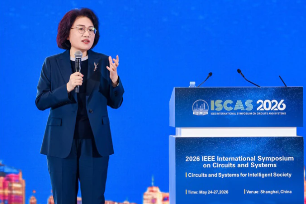
The Huawei chip breakthrough 2026 is the most significant semiconductor announcement from China since the Mate 60’s 5G chip surprised the world in 2023. At the 2026 IEEE International Symposium on Circuits and Systems in Shanghai on May 25, He Tingbo — president of Huawei’s semiconductor business — delivered a keynote titled “New Semiconductor Path in Practice,” unveiling what the company calls the Tau Scaling Law, a proposed replacement for Moore’s Law that uses 3D chip stacking rather than transistor miniaturization. The breakthrough, which Huawei says will deliver transistor density equivalent to 1.4-nanometer processes by 2031, has generated 40 million views on Chinese social media under the hashtag “Huawei Semiconductor Field New Breakthrough” — and a remarkable concession from Nvidia’s CEO delivered just days earlier.
Why Moore’s Law Matters — and Why China Can’t Follow It
To understand the Huawei chip breakthrough 2026, you need to understand the problem it claims to solve. Moore’s Law — the observation by Intel co-founder Gordon Moore that the number of transistors on a chip doubles roughly every two years — has guided the semiconductor industry for more than five decades. The law works by shrinking transistors so that more fit on the same silicon area.
The problem for China is that shrinking transistors requires extreme ultraviolet lithography machines — EUV — which are produced almost exclusively by ASML in the Netherlands. The United States, Netherlands, and Japan have jointly prohibited the export of EUV machines to China since 2023. Without EUV, China’s most advanced chipmaking capability is currently thought to be around 7 nanometers. Taiwan’s TSMC — which makes chips for Nvidia, Apple, and AMD — is manufacturing at 2nm and plans to start mass production at 1.4nm in 2028.
That gap — 7nm in China versus 1.4nm at TSMC — is what the Tau Scaling Law claims to address through a fundamentally different approach that does not require EUV machines.
The Tau Scaling Law: Time Replaces Size
The Huawei chip breakthrough 2026 announcement introduces a new principle that He Tingbo says replaces geometric scaling with time scaling as the guiding metric for semiconductor evolution.
The proposal is as follows: instead of measuring progress by how small you can make transistors, measure it by how fast signals can travel through the chip. The Greek letter tau (τ) represents the time constant — the time it takes a signal to propagate from one point in the circuit to another. Huawei’s thesis is that reducing τ produces performance improvements equivalent to shrinking transistors, without requiring the lithography machines that produce smaller transistors.
He Tingbo formally presented this as the “Tau Scaling Law” — which Chinese social media users have nicknamed “Her’s Law” in reference to He’s gender and the innovation’s origin. The Tau Scaling Law proposes replacing geometric scaling with time (τ) scaling as a new guiding principle for the evolution of both semiconductors and electronic systems. Based on this principle, innovative technologies such as LogicFolding can be used to continuously compress signal propagation delay and steadily improve transistor density.
LogicFolding: 3D Vertical Stacking as Moore’s Law Alternative
The practical implementation of the Huawei chip breakthrough 2026 is a technology called LogicFolding. Rather than shrinking transistors into the flat 2D plane of a silicon wafer — which is what EUV lithography enables — LogicFolding folds traditional 2D circuits into 3D vertical stacks, essentially building skyscrapers out of chip layers.
He Tingbo described it at the IEEE ISCAS keynote as adopting the LogicFolding architecture to break down the physical boundaries of traditional circuit layouts, significantly shortening critical-path wiring, effectively reducing the resistive and capacitive load of signal propagation, and ultimately boosting transistor density and circuit performance.
The engineering logic is sound in principle. Stacking layers of transistors vertically can increase the density of transistors per unit of horizontal silicon area — achieving some of the performance gains that transistor miniaturization provides, without requiring the miniaturization itself. Samsung and TSMC are both working on similar 3D stacking approaches, though for different reasons. Huawei’s version is specifically designed to work within the EUV prohibition that China faces.
The Numbers: 1.4nm by 2031
The specific claim at the center of the Huawei chip breakthrough 2026 is a performance target. By 2031, the high-end chips Huawei designs based on the Tau Scaling Law are expected to feature a transistor density that is equivalent to 14 Angstrom (1.4 nm) processes.
TSMC, the world’s most advanced chipmaker, plans to start mass production of 1.4nm chips in 2028. If Huawei achieves its 1.4nm-equivalent target by 2031, China would be approximately three years behind the global frontier — a dramatically compressed gap from the current 5 to 7 year deficit at the manufacturing level.
The Kirin chips scheduled to launch in Fall 2026 will be the first ever to adopt the LogicFolding architecture. Over the past six years, Huawei has designed and mass-produced 381 chips based on the Tau Scaling Law’s foundational principles, serving a wide range of industries, sectors, and markets.
Jensen Huang’s Remarkable Concession
The context for the Huawei chip breakthrough 2026 announcement includes one of the most significant statements Nvidia CEO Jensen Huang has ever made about the Chinese market. Huang told CNBC last week that his company had “largely conceded” the Chinese AI chip market to Huawei.
Huang traveled with President Donald Trump to China this month for a summit with Chinese leader Xi Jinping. After the Nvidia CEO’s CNBC interview — in which he acknowledged Huawei’s dominance in the Chinese chip market — he suggested in Taiwan that China would still be a significant source of long-term demand, telling reporters that China was part of the $200 billion market he had forecast for Nvidia’s new Vera central processing units.
The United States had approved Nvidia’s H200 chip for export to certain Chinese companies under conditions established late last year, but no orders have been made. The combination of Huang’s “largely conceded” statement and Huawei’s Tau Scaling Law announcement on the same weekend creates a narrative of Chinese semiconductor momentum that would have seemed implausible two years ago.
The “DeepSeek Moment for Chips”
Chinese social media’s response to the Huawei chip breakthrough 2026 announcement was immediate and intense. On Chinese social media platform Weibo, the hashtag “Huawei Semiconductor Field New Breakthrough” generated 40 million views. Some commenters described it as the “DeepSeek moment” for China’s chip industry, referring to an AI model released by a Chinese startup that was said to match or outperform leading American models at a fraction of the cost. Others said U.S. sanctions had encouraged Chinese innovation.
The DeepSeek comparison is instructive. DeepSeek surprised the world by achieving frontier AI performance through architectural innovations that reduced the compute requirement — effectively working around the hardware constraint that US export controls imposed. Huawei’s LogicFolding claims a similar route: architectural innovation around the hardware constraint of EUV unavailability.
Whether both analogies hold in practice is the question the industry will spend the next five years evaluating.
The Skeptics: Challenges Remain Real
The Huawei chip breakthrough 2026 announcement was met with cautious analysis from semiconductor industry observers outside China. Brady Wang, associate director at Counterpoint Research, noted that “cost, power, heat and system integration remain major challenges” for Chinese tech.
He Tingbo acknowledged these limitations directly in her keynote. The traditional tools are not yet sufficient for full-scale free logic design, she said, and thermal management remains a critical issue since the components are stacked vertically. Heat management in 3D stacked chips is a genuine engineering challenge — when you stack transistors vertically, heat generated in lower layers has difficulty dissipating through the layers above it. That thermal constraint limits how many layers can be stacked and how hard they can be driven.
Wang told Reuters that “in the short term, China may narrow the gap with global leaders, but a technology gap with the most advanced nodes will still remain.” The gap may compress from today’s 5 to 7 years to 2 to 3 years — meaningful progress, but not full parity.
Broader Implications: What the Tau Law Means for the AI Chip War
The Huawei chip breakthrough 2026 announcement is the clearest signal yet that China’s semiconductor industry is not simply trying to replicate the Western approach within export control constraints. It is trying to develop an alternative approach that makes those constraints irrelevant.
If LogicFolding delivers its promised performance gains at scale, the US export control strategy — which is predicated on the assumption that cutting off EUV access permanently hobbles Chinese AI chip capability — may need fundamental reassessment. The strategy assumed that Moore’s Law scaling through transistor miniaturization was the only viable path to cutting-edge performance. Huawei is betting that it is not. For more on the biggest stories in technology, semiconductors, and global AI competition, visit The Tech Marketer.
Latest Updates
The Huawei chip breakthrough 2026 was announced at IEEE ISCAS Shanghai on May 25. Here is where to follow the full coverage:
- CNBC has the full analysis of Huawei’s new smartphone chip plans for Fall 2026 and the broader context of Huawei’s rivalry with Nvidia and Apple in the AI chip competition, including Jensen Huang’s “largely conceded” market statement from the same week. Read more at CNBC
- NBC News has the complete report on Huawei’s chip design breakthrough including the Tau Scaling Law explanation, the 1.4nm 2031 target versus TSMC’s roadmap, Jensen Huang’s comments, Brady Wang’s Counterpoint Research analysis, and the Chinese social media response calling it a “DeepSeek moment.” Read more at NBC News
- Huawei’s official announcement has the complete technical details of the Tau Scaling Law presented at IEEE ISCAS 2026, including the LogicFolding architecture specifics, the four-level optimization mechanism from device to system, the UnifiedBus SuperPoDs system integration, and the 381 chips mass-produced using Tau Scaling principles. Read more at Huawei
FAQ: Huawei Chip Breakthrough 2026
1. What is the Huawei Tau Scaling Law chip breakthrough? At the IEEE International Symposium on Circuits and Systems in Shanghai on May 25, 2026, Huawei semiconductor president He Tingbo unveiled the Tau Scaling Law — a proposed replacement for Moore’s Law that uses time (signal propagation delay) rather than transistor size as the guiding metric for chip performance improvement. The approach uses a technology called LogicFolding to stack circuits in 3D vertical layers instead of shrinking transistors on a 2D plane, bypassing the need for EUV lithography machines that China cannot access under US sanctions.
2. What performance does Huawei claim for its new chip technology? Huawei claims that by 2031, its high-end Kirin chips designed using the Tau Scaling Law will achieve transistor density equivalent to 1.4-nanometer processes. For comparison, TSMC — the world’s most advanced chipmaker — plans to start 1.4nm mass production in 2028. China’s current most advanced chip manufacturing capability is thought to be around 7nm. The first chips using LogicFolding architecture are the Kirin chips launching in Fall 2026.
3. What is LogicFolding and how does it work? LogicFolding is Huawei’s 3D chip stacking architecture that folds traditional flat 2D circuit designs into vertical layers — essentially building upward instead of shrinking inward. By stacking circuit layers vertically, Huawei aims to increase transistor density without requiring the extreme ultraviolet lithography machines that traditional transistor miniaturization requires. The approach shortens critical-path signal wiring, reduces resistive and capacitive load, and boosts transistor density and circuit performance.
4. What did Jensen Huang say about Huawei and the China chip market? Nvidia CEO Jensen Huang told CNBC last week that his company had “largely conceded” the Chinese AI chip market to Huawei. Huang made the comment after traveling with President Trump to China for a summit with President Xi Jinping. Despite the concession on the Chinese market, Huang separately said China remains part of the $200 billion market he has forecast for Nvidia’s new Vera CPU product line.
5. What are the challenges facing Huawei’s chip breakthrough? He Tingbo acknowledged that traditional chip design tools are not yet sufficient for full-scale LogicFolding implementation and that thermal management is a critical issue — heat generated by lower stacked layers has difficulty dissipating through upper layers. Counterpoint Research analyst Brady Wang noted that “cost, power, heat and system integration remain major challenges” and that while China may narrow the gap with global leaders, “a technology gap with the most advanced nodes will still remain” in the short term.
Sources and References
- CNBC: Huawei Plans New Smartphone Chips This Fall as Rivalry With Nvidia and Apple Intensifies
- NBC News: China’s Huawei Touts Chip Design Breakthrough in Bid to Defy U.S. Sanctions
- Huawei Official: HUAWEI Presents the Tau (τ) Scaling Law, Enabling Breakthroughs in Transistor Density and System Performance